(pronounced Tun-e-far)
Version 2.0 - This version of the documentation was last changed on June 3rd.
IMPORTANT: you need a soldering iron with the finest tip you can find and use very fine gauge solder - if you don't have these go out and buy some solder and a new tip for your soldering iron right away - read all these instructions and make sure you understand them before starting
Parts List:
Flight Computer V1.0:

B1	PC Board
U1	80C32			microprocessor
U2	27C256-12		32Kx8 ROM - 120nS "V2.1"
U3	74HC373
U4	LM340T-5		5v regulator (might be a 7805 part)
U5	43256-15		32Kx8 RAM - 150nS
U6	74HC00
T1-T4	2N6045 or 2N6044	darlington output transistors
Y1	11MHz			crystal
S1	28-pin socket		ROM socket
R1	8k2			reset pullup
R2	90-120 ohms		charge reservoir fill rate
R3-R6	10k
C1-C2	30 or 33pF
C3	10uF
C4	100uF			power decoupling
C5	0.1uF			power decoupling
C6	1000uF			charge reservoir
C7-9	0.1uF			power decoupling
P1	6 pin connector		main connector
P2	10 pin header socket	aux connector
P3	3 pin header socket	serial connector

RS232 interface:

U100		RS232 level converter - MAX232 or equiv.
C100-C104	10uF capacitors
P100		RS232 connector for your computer
P101		small connector to match P3 above (included in the FC kit)
Note that there should also be plugs to match all the connectors on the flight computer and a bag of pins for the plugs - they are very small so be careful you don't lose them. P1 is a 0.156 (really 4mm) pitch molex connector available at many local electronic supply places - P2, P3 are 2mm DF3 connectors by Hirose Electric available from DigiKey.
A number of the components - in particular the TO220 transistors and the crystal may have bent leads - straighten them out - they are intended to be placed vertically.
As usual you should observe care with static sensitive parts - only remove them from their tube just prior to using them and always gently ground yourself and your soldering iron tip prior to working with any parts.
This board is designed to work with any of the 40-pin 8051/8031/8052/8032 variants of microprocessors - I've chosen the 80C32 mostly because it's available and because it runs at a much lower power than the plain 8051/8031s that are more commonly available (15mA vs 160mA).
The PCB is double sided with plated through holes. It has rather fine traces - take great care not to bridge these use as little solder as you can - too much heat can cause them to lift or damage the thru-holes - try using a soldering iron with the finest tip you can find (1/32 for example) and spend the smallest amount of time possible soldering each pin. Too much heat can cause traces to lift or the plating through to fail (all the holes on the board contain metal that connects the pad on the top with the one under it - many of the small holes you see on the board are 'vias' - holes used purely to connect a trace on the top to one on the bottom of the board.
The 11mHz crystal can be replaced with a 12MHz one, or even a 16MHz one (if you have an 80C32-1) - but I've used 11MHz because the serial baud rates work out right with the simple timers. In other words the supplied rom will stop working and you will have to provide your own.
The ROM is socketed, I'll provide already burnt ROMs containing a monitor, Basic and Forth that will talk to the serial port at 9600 baud - this monitor only works on 8032/8052 and variants (it uses the upper 128 bytes of on-board SRAM for a buffer).
I've tried to write this document so that it has information for people with a whole range of experience building electronic gear - you may find parts of it too wordy - or too difficult or confusing - I'd appreciate feedback to help me make it better. This page is rather long - I wanted to make it easy to print out a copy.
Construction
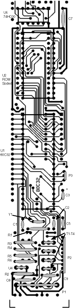
Assembly can be done in 1/2 an hour, I suggest you take your time and go as slowly as possible. A component placement diagram is located after the assembly instructions below.
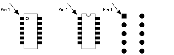
Notes: pins on chips are numbered counter clockwise. If you look at the top of a chip (with the pins facing down one end will have a notch or a dot - the dot indicates pin number 1, the notch indicates the top, if you orient the chip with the notch up pin 1 is at the top left next to the edge with the notch. On this board pin 1 always goes into a square pad.
Assembly instructions:
Before you continue you should check out the section below describing options you can make to the board.
The following is the bottom portion of the upper side of the board showing component placement:
The following is the bottom portion of the lower side of the board showing component placement:
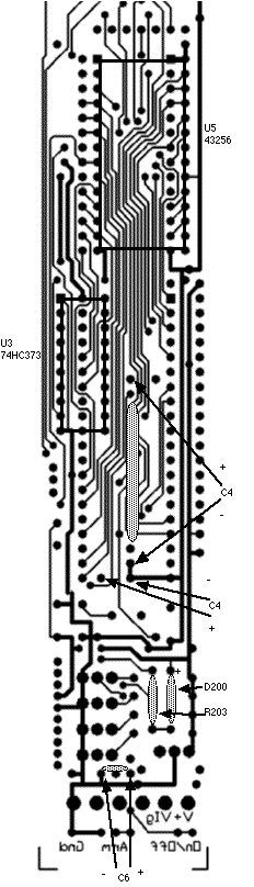
Note the locations of the pads for the pins of C4 and C6 are shown using arrows. Two possible locations for C4 are shown because two different packaging styles for this capacitor have been shipped in various kits - use the one that's appropriate for your part. Also D200 and R203 are optional and not included in the kit - they are included in this diagram so you know where to put them should you choose to add them as described below.
RS232 Converter
Next assemble the RS232 converter ..... if you need one - this inverts the serial signals and level shifts them to RS232 levels and is able to drive a wire long enough to get safely away from a launch pad :-) This whole area has lots of scope for you to do things your own way - I've explained how I did it - you get to choose one that's right for you.
I haven't included a circuit board for this piece of logic ... just buy a simple prototyping board from Radio Shack, or rats-nest it in place, the basic circuit is:
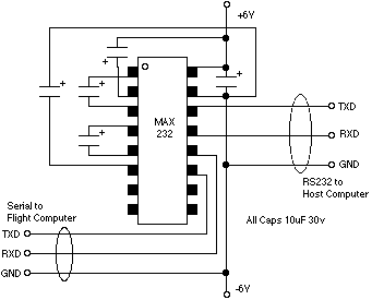
Notice that all the capacitors are polarized and it's important you get them the right way around. In the diagram the MAX232 is shown from above. Be careful you connect the correct contacts to the flight computer - you WILL damage it if you wire up the RS232 side to the flight computer.
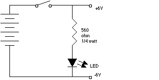
I packaged mine in a small box containing a battery holder for 4 C cells, a slide switch and an LED
The +/-6V terminals in the above diagram are where the 6v power supply is connected - -6v is really GND (it's not a dual voltage supply).
The side marked "Serial to Flight Computer" should be connected to the 3-pin plug in the order shown on the above diagram and plugged in to the 3-pin header on the right hand side of the computer - see the section on connector P3 about how to wire this end correctly. The RS232 pins have to be connected to your host computer - how this happens depends on how your computer is wired you should have told me what sort of connector you wanted when you ordered the RS232 kit. In my box I put a mini telephone connector on the side so I can use a normal telephone extension cord to extend the distance from the box by several hundred feet if I want to. I wired the GND to the yellow line, TXD to the black line and RXD to the red line. I bought a 3ft telephone extension, chopped one end off and wired a plug for my computer onto it. (You have to be careful - telephone connectors gaily swap black-yellow, red-green so follow it through). If you do this don't plug it into the wall telephone socket you'll blow something up :-).
Here's how to wire some familiar types of computer, if your's is not here get in touch and I'll try and talk you through making a cable for yours:
Mac
Macs use a mini-DIN 8 connector (the plug) - these have to be one of the most annoying, fiddly god-forsaken pieces of hardware to solder ever designed ..... you only have to do one. Look closely at the plug and how it goes together - don't forget to put the outer connector sleeve over the cable you are soldering before you start, the connector (viewed from the side you are soldering) looks like:
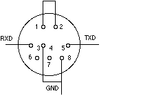
Be careful soldering the back of this connector the plastic it's made of is pretty easy to melt. When you are done wrap some tape around the wires before you put the shield back on so it can't short out.
PCs
I only know how to wire the 9-pin DB9 connectors (connectors usually have the pin numbers molded in them):
General RS232 Connectors
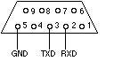
Here's how to wire your generic DB25 connector (connectors usually have the pin numbers molded in them):
Note that for almost every machine there's something different - the usual thing to do if something doesn't work is to swap the RXD and TXD wires and see if that fixes it.
Bring up
Hook up the flight computer to a 9V battery (make sure you get it the right way around - the positive terminal should be wired to the left hand pin on the bottom connector, the negative terminal should be wired to the right-most pin of the same connector - with a multi-meter quickly measure the current draw - it should be ~40mA - if it isn't disconnect it quickly. Gently touch each of the chips or transistors on the board - if any of them are hot to the touch - disconnect quickly - if either of these problems happen inspect the board - are there any solder shorts? open connections? chips in backwards?
If you have a 'scope check out pin 39 on U1 (the 80C32) you should see data moving here.
Now hook up the serial connector and plug in the host - run a terminal program and set it up for use with a direct connection (no modem) through the serial port you connected to. Set the baud rate to 9600 baud - 8 bits, no parity, 1 stop bit. Turn on the flight computer - you should see a startup message followed by a prompt (yes that is the prompt :-). Type '?
If nothing happens disconnect the RS232 converter - short the RXD and TXD pins going to the flight computer - try typing in your terminal emulator on your host - what you type should get echoed - if not there's something wrong with the converter. Unshort them - echoing should stop.
Again now is a good time to look for solder shorts, opens or components that are in the wrong place or backwards.
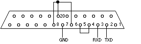
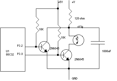
P1 the main connector
Note: in the following docs P3.0-7 and P1.0-7 refer to bits in the parallel ports
on the CPU that you can set or read from software. There are 4 8-bit ports P0-P3 and individual bits in them are refered to by their bit index.
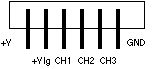
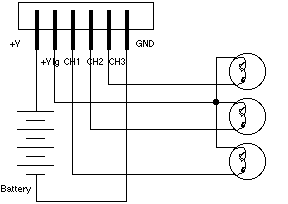
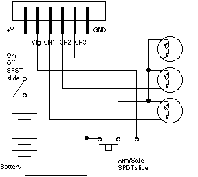
This connector is the main one at the bottom of the board it has 6 pins, looking from the upper side of the board:
You connect +V to the positive terminal of a 6V-12V battery, GND is the ground, +VIg is the common wire for all the igniters and CH1, CH2 and CH3 are individual igniter (ie flashbulbs or electric matches) wires. CH1 is driven by P3.3, Ch2 by P3.5 and CH3 by P3.4
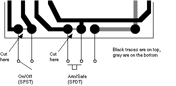
Or a wiring harness with more stuff (an on/off switch and an arm/safe switch):
The actual circuit for each igniter looks more like:
When P3.X is turned on the internal pullup and the 10K resistor drive the transistor that sinks the contents of the capacitor through the flashbulb/electric match. If you want more reliable ignition you can use a bigger capacitor. The capacitor is shared by all the igniter circuits so you should only fire one at a time and let it have enough time to recharge (say 1 sec) between uses. P3.2 is the arm circuit - P3.2 must be at 0 for the capacitor to charge - and you must arm
the circuits about a second before they can be fired - note that at reset the 80C32 automatically discharges the capacitor because all the P3.X outputs are driven.
The 120 ohm resistor is so that the instantaneous short of firing an igniter doesn't deprive the CPU of power. Notice that the capacitor is charged to the full voltage of the supply battery, not the lower regulated supply of the CPU - for this reason a 9v or 12V supply is better than a 6V one.
A quick note about wiring harnesses - you make soldered or crimped connections
for one purpose only - to make electrical contact - they should never be used to
support the weight of wiring or any other component especially under G loadings
- always use strain relief
(epoxy the wiring to the body tube or something).
You should always ground test your electronics and software before flying
it - toast a few igniters or flashbulbs before you waste an airframe.
P2 - the auxillary connector
Connectors
P3 - the serial connector
Options
There are a number of options on the board - you may see stray pads or traces and wonder about their purpose - here are as many as I can remember ....
Proto area
The proto area at the top is not wired to anything except for the pads in the center of the IC area - the ones with the traces on the upper side of the board are +5V, the ones connected to the shorter traces on the bottom are GND.
Reset switch
If you are doing software development having a reset switch is very useful - you can add one by connecting a SPST switch between pin 9 on U1 (there's a free pad sitting there) and +5V on the board (there's a via just to the left midway between pins 4 and 5 of U1 that you can use). Or you can connect the switch across C6.
On/Off switch
At the bottom of the board is a pair of pads that can be used to wire up an on/off switch - just cut the thin trace on the bottom then wire a slide switch between the pads. Or you can install the on/off switch into the wiring harness connected to P1 as described above.
Diode protection
If you didn't install the above switch you can still cut the trace and install a small power diode (1N4001 or equivalent) between these two pads (put the banded end of the diode to the right) to protect the flight computer from you wiring it up backwards.
Arm Switch
There are 3 pads at the bottom which can be used to wire a safe/arm switch into the circuit - it shorts the igniters in one position and arms them in the other. Even though there is a software driven arm mechanism onboard this is a case where "belt and braces" is a good thing. Another way of wiring an arm switch (into the wiring harness) is shown above.
Parallel ports
All the pins on P0 and P3 are brought out to pads on the LHS of the board, there are a number of power and ground pins hanging around there too if you want to use them (the power pins are directly above and below the parallel port pins, the grounds are indented a little near U1's pin 1).
Leaving things out .....
One or any of the transistors and their pullup resistors can be left off the board.You can also cut off the metal tab at the top of the transistors or the voltage regulator to save weight.
If you have a 6V supply you should replace the voltage regulator with a small power diode (1N4001 or eqv.) with the positive end in the rightmost pad of the regulator and the negative end in the leftmost (leave the middle one alone) this diode provides the required voltage drop and also provides protection against plugging the battery in the wrong way around. Don't try this if you have a supply of more than 6V.
You can leave off the ROM if you have an 8052 or 8051 etc with internal ROM, if you do this there is a small ground trace next to U1 pin #31 which should be cut and a pad underneath the 80CXX that should be tied to +V.
You can leave off the RAM - if you do you can also leave off the 74HC00 - but you must jumper pin 1 of the 74HC00 to pin 11.
You can (carefully) cut off the proto area at the top, after you do so make sure that none of the power or ground traces that go up there are shorted.
Additional Circuitry
This section is only for the V2.0 boards - it describes how to add the additional circuitry for which there are pads at the top of the board. You should NOT do this untill you have got the kit built and running, add these components one set at a time and after each one make sure that everything is still working. The circuits for all these are on the third sheet of schematics
Serial EEPROM
This consists of a serial EEPROM into which your software can store data and it will stay there even if the battery goes flat (for example if it takes a couple of days to find your rocket ....). Or you can preprogram parameters or code into one and add it to your machine in the field and use ROM based code to download it at poweron time. The ROM we're using is a 16kbit 24LC164/P from Microchip Technology - these are relatively slow ROMs - and you can't execute code directly out of them (but you could copy it to sram)- they are available for $2.19 from DigiKey (1-(800)-344-4539 - or at http://www.digikey.com/.
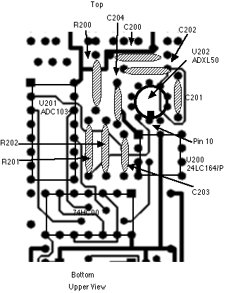
Parts List:

	U200	 	24LC164/P
	S200		8-pin DIP socket
	C200		0.1uF DC
To install one on the board you need to also buy an 8-pin DIP socket and a 0.1uF disc ceramic capacitor. Install the socket directly above the 0.1uF capacitor to the right of the 74HC00 at the top of the board. Like all the rest of the parts on the board install it with the notch facing the top of the board. Also install C200 a 0.1uF capacitor in the location shown on the diagram below just below the proto-area at the top of the board.
If you have a Version 2.0 board (look underneath at the top - then there is a slight bug on the board - pin 7 of the 24LC164 needs to be grounded, run a wire cross to pin 2
Analog to Digital Converter
This part is an ADC1034CIN-ND - a 4 channel 10-bit serial ADC, $9.58 from DigiKey (see above) it's made by National Semiconductor.
Parts List:

	U201		ADC1034CIN-ND
	C200		0.1uF (same as above)
Install the ADC in the pads on the far left side of board directly above the 74C00 again the notched end (pin 1) faces the top of the board. You must also install the 0.1uF decoupling capacitor as described above (but obviously only once if you install the eeprom too).
Note: channel 3 of the ADC is hardwired to the output of the ADXL50 accelerometer. Channels 0-2 are connected to the three pads visible directly above the ADC. Underneath the board these 3 pads are shorted to ground. If you wish to use one of these inputs take a sharp modelling knife and cut the trace under the board just above the pad.
ADXL50JH Accelerometer
This part is a +/- 50G accelerometer - made by Analog Devices. It is not cheap - roughly $19 available from Allied Electronics (800)433-5700 or Newark Electronics (312)784-5100. To use it you must also have the ADC described above installed.
The sensor is in a TO-10 (round) can - it is soldered into the ring of 10 pads just above where the EEPROM socket is soldered - there is a tab next to one pin and this pin must go down - on the pad to which that pin is to be soldered, on the underneath side, there is a small tab that can be seen by turning the board upside down. The acceleration axis that the sensor measures is along the long axis of the PC board.
Parts List:

	U202		ADXL50
	C201		0.1uF
	C202		0.1uF
	C203		0.1uF
	C204		0.1uF
	R200		49.9k		51k
	R201		105k		100k
	R202		274k		270k

(note all resistor values 1% tollerance - the numbers on the left are
ideal, the ones on the right easily obtainable)
Install the resistors and capacitors as shown in the diagram below.
R/C In
There are pads on the underside of the board underneath the 4 10k resistors down near P1 the power connector for adding the resistor and diode that are required to listen to an R/C receiver.
Parts List:

	D200		small signal diode 1N4001 for example
	R203		330 ohms
The location of these two parts is shown on the main component placement diagram back at the end of the main assembly section. Make sure you get the diode in the right way around - the end with a colored band should go to the pad marked "+".
Memory Map
The processor has 3 separate memory spaces:
Internal RAM - there are 256 bytes of this and most instructions can reference it directly, the upper 128 bytes of it are overlaid by the processor registers - check out an 8051 reference manual for more information about this.
Program memory - there's 64K of this - some of it can be on-chip in some 805X variants - our 80C32 has none on-board. Data can be read from this using a movc instruction.
External data memory - there's 64K of this too - data can be read and written from this memory using a movx instruction.
In this design the program and external data memory spaces have been unified, the lower 32K is the ROM, the upper 32K is the RAM, instructions can be executed from the ROM or RAM and data can be read from either or written to the RAM. Just over 3/4 of the ROM is actually used for the software you are free to drop whatever you like in the rest - but remember that future versions may use more of this space. A Unified space means that the movc and movx instructions access the same memory - and that you can execute code out of SRAM.
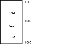
The interrupt vectors in low ROM are vectored through locations in internal RAM so you can locate interrupt service routines in external RAM.
If you program in assembly then all of the external RAM is available to you, the ROM monitor uses none of it. If you use Forth or Basic they take care of allocating RAM space.
Peripheral Ports
The processor has a large number of peripheral ports (32 of them) however many are used already in this design:
The remaining 12 bits are available for use - P3.2 is wired to the safe/arm circuit, P3.3-P3.5 are wired to the pyro circuits (but don't have to be used for this purpose), P1.6-P1.7 are also wired to the aux. connector P2.
For safety's sake the processor comes up with port P3.2 asserted - this shorts all the pyro outputs - to arm the pyro drivers clear P3.2 it takes about a second for the capacitor to charge so you must do this at least a second prior to firing one of the pyro drivers (for a similar reason you must wait at least a second after firing one channel before firing another). A good time to arm might be at liftoff, or when you detect burnout. There is one downside of this mechanism - the shorting transistor sucks quite a bit of current when it's safed - if you have a battery with a short lifetime you may want to have your software arm the channels once it's been loaded on the pads. Because of the way that the 80C32 resets it's important that you do NOT disconnect the safe/arm circuit because otherwise a cpu reset (or power on/off cycle could cause a pyro event) - for added protection add an external safe/arm switch as well as shown above.
To read a bit in a port you must have written a 1 to it. All ports have active pull downs and weak pull ups. The value read is the external logic level, if you have a 1 written into a port but there is a large external load (for example one of the pyro driver transisters) you will still read it back as a 0.
P1.0-P1.4 are used to communicate with the serial A/D and NVRAM circuits access routines for them are provided in the rom.
In assembler you can read or write all 8-bits of a port using a move instruction:
		mov	P3, abcd
		mov	P3, #0x56
		mov	a, P3
Or you can read or write a single bit:
		mov	c, P3.4
		setb	P3.5		; this one fires a pyro charge if it's armed
		clr	P3.6
		jb	P1.6, label
		mov	P1.0, c
		mov	c, P1.0
In Basic you can change a port by:
	LET P3 = 56			; sets a whole port
	LET P1B(4) = 1			; sets bit 4 in port 1
	LET B = P1			; reads a whole port
	LET B = P3B(4)			; reads a bit in port 3
In Forth you can read the contents of a port or register or a bit in port or register using:
	?P3		returns port P3
	?P1_6		returns bit 6 of P1
and you can write a port:
	P3!		writes the value at the top of stack to P3
	P1_6!		write the value at top of stack to bit 6 of P1
So you can use the following code to fire a pyro charge:
In assembly

	clr	p3.2				; arm it
..... (at least a second later)
	setb	p3.5				; fire it
L1:						; set the timer
	mov	tcountl, #1000&0xff
	mov	tcounth, #1000>>8
	mov	a, tcountl
	cjne	a, #1000&0xff, L1
	mov	a, tcounth
	cjne	a, #1000>>8, L1
L2:	mov	a, tcounth			; timeout
	jnz	L2
L3:	mov	a, tcountl
	jnz	L3
	clr	p3.5				; clear it

In Basic

50	LET ARM = 1				arm it
.... at least a second later
100	LET P3(5) = 1				fire it
101	FOR I=1 TO 100				wait some time
102	NEXT I
103	LET P3(5) = 0				clear it
104	LET ARM = 0

In Forth

	1 ARM					arm it
.... at least a second later
	1 P3_5!					fire it
	1000 IWAIT1MS				wait 1000mS (ie 1S)
	0 P3_5!					clear it
	0 ARM
Note that in Basic "ARM = 1" is the same as "P3(2) = 0", and in Forth "1 ARM" is the same as 0 P3_2!"
The drivers for the (optional) ADC1034 are included in the ROM, they are accessable through the low core utility vector:
get_adc:
        mov     r2, #'A'
        mov     r1, #utility_vector
        mov     a, @r1
        mov     dpl, a
        inc     r1
        mov     a, @r1
        mov     dph, a
        clr     a
        jmp     @a+dptr
Now call get_adc with the channel you want (0-3) in r0, the result
is returned in r1:r0 - the ADC1034 is a 10-bit ADC so the 6 lsbs of
r0 are returned as 0 (this way you can replace the driver in the
utility vector chain with one for a 16-bit ADC and get a meaningfull
result.Note that analog channel 3 is by default connected to an ADXL50
In Basic you can access the ADC by reading ALG(n) (n=0-3).
In Forth the you can read the 4 analog channels by "?A0", "?A1" etc
Software
There's quite a lot of software I'm shipping with the board, some of it is designed to go in ROM, some of it's development software etc etc. All the sources are included you are welcome to hack on them to your heart's content. Some software contains my copyrights, I always do this to protect myself should I wish to sell the software in the future. Some of the other software (the Basic and Forth) are from public domain sources on the net - they contain information about their authors in their source.
There are 4 main pieces of software I'm currently shipping - sources and/or binaries are on the sources page:
This is what you see whenever the flight computer is reset, it prompts ":-) " and accepts the following commands:
A 0-3 displays analog channel n (ADC1034 must be installed) ARM +/- arms/disarms the pyro charges (disarmed at reset) DC addr display program memory DM addr display external memory DR addr display internal memory SM addr ... set external memory SR addr ... set internal memory G addr make a subroutine call to that address I addr disassemble the code at that address IL addr disassemble a page of code at that address R dump the registers : data download an Intel hex record (they all start with ':') T enter Basic F enter ForthThere's also a number of very basic system services provided to environment, including setting up some basic registers (the serial port and timer 1 as a baud rate generator for it), a timer (timer #2) providing a 24-bit real-time clock that is always running in internal SRAM, interrupt call backs etc.repeats the last display command
What follows is only of interest to those who want to program the computer in assembler.
You can always write code that takes over the machine and ignores the monitor, if you want to coexist with it then you have to keep out of its way (Tiny Basic and Forth do this the only way to get back from them is to power cycle them or reset the CPU).
Here's a list of internal SRAM locations are used by the monitor -
The following addresses contain pointers to interrupt service routines, the ROM ISRs always vector through these addresses:
vint0 		0x30		interrupt 0 vector
vint1		0x32		interrupt 1 vector
vtint0		0x34		timer interrupt 0 vector
vtint1		0x36		timer interrupt 1 vector
vtint2		0x38		timer interrupt 1 vector
vser		0x3a		serial interrupt vector


timel 		0x3c		time counter - this 24-bit counter is incremented every clock tick
timem		0x3d		(millisecond) to sample this copy (in order) timeh, timem, and timel
timeh		0x3e		to somewhere else then check that timeh and timem haven't
				changed, if they have start again repeat until you get it (remember
				you are synchronizing with an asynchronous interrupt

buffp		0x3f		used internally

tcountl		0x40		counts down every tick and stops at 0 - set it and wait
tcounth	0x41			until it hits 0 to wait for a known amount of time.
				the correct way to write this is to write 0xff to tcountl,
				write the upper bits of the number you want to tcounth, then
				write the lower bits of the number you want to tcountl.
The following can only be accessed via @Ri - they are vectors for call back to the monitor, you can use code like the following to call through them:
mov r0, #poll_vector mov a, @r0 mov dpl, a inc r0 mov a, @r0 mov dph, a clr a jmp @a+dptr poll_vector 0x80 pointer to serial poll routine - when called returns a character in A if one is available or 0 if not idle_vector 0x82 pointer to idle routine - you can install something here if you want to do stuff while the monitor is waiting for characters cli_vector 0x84 pointer to cli routine - this routine is called with characters in the buffer whenOnce we standardize on NVRAM and A/D interfaces I'll probably add internal service routines that will provide access to these.is typed - you can add your own if you like or use it to add more commands (hacking a ROM might be easier) send_vector 0x86 pointer to send routine - calling this sends the character in A out the serial port prompt_vector 0x88 pointer to prompt routine - prints the prompt utility_vector 0x8a pointer to utility routine - how we will add ROM-based drivers in the future old_addr 0x8c used internally old_type 0x8e used internally buff 0x8f used internally
The monitor runs with Timer 2 interrupts enabled and all others disabled.
Basic
The Basic is simple and slow all math is done in floating point ... it comes from Intel - much of it is intended for a particular hardware environment that is different from ours - I've removed most of the commands for that environment.
I'm still hoping to track down a manual for it, so far I've had no luck.
Strings in this variant of Basic are a little wierd - before you can use them you have to allocate space using "string NNN, MMM" where NNN is the amount of space you are allocating to all the strings and MMM is the size of each string. " The "string" command also does an implicit clear - so do it first before loading in your program. Strings are not named "a$" etc instead they are numbered as "$(0)", "$(1)" etc etc.
Other built-ins include commands "PH0." and "PH1." for printing things in hexadecimal - for example "ph0. p3" prints out port 3 in hex.
I've added the following things for accessing the hardware:
Forth
Enter Forth by typing "f
The Forth is pretty simple - it's all 16-bit. I've made the following enhancements:
A copy Of Julian Noble's Forth primer is available here. And a Forth home page is also available.
Assembler
The assembler is something I wrote a few years ago it's in vanilla C/yacc source and has been ported to various machines - I'll make sources, as well as Mac and PC binaries available.
Sources and binaries will be available on the flight computer sources page at http://www.taniwha.com/~paul/fc/srcs.
The assembler accepts pretty normal 8051 assembler syntax with a few wierdities:
To create downloadable code you need to start the code at somewhere that will actually have sram at it (ie >= 0x8000). What follows is a simple piece of code that calls back to the monitor to send characters:
There are a couple of other examples available - firstly the code for the box I use to sequence the hybrid launchers - it's at http://www.taniwha.com/~paul/fc/srcs/hybrid.s and the monitor/basic/forth source for the ROM which is at http://www.taniwha.com/~paul/fc/v2.0/ostbef.s.
Required reading in order to program an 805X in assembler is the Intel data book '8-bit Embedded Controller
Handbook' 1991 or later (ISBN 1-555-12-121-7, Intel #270645) - you can probably get
it from your local electronics supplier or call Intel at (800)548-4725. The latest ones come in two volumes make sure you get the one that contains just the 805X programming info.
8051 documentation on the Web
Class notes for a community college class that uses 8051s for teaching oriented around a Phillips variant:
http://www.cit.ac.nz/smac/cbt/hwsys/i8051/default.htm
A set of pages referencing stuff all over:
http://livewire.ee.latrobe.edu.au/~sjm/
Basic52 documentation and stuff:
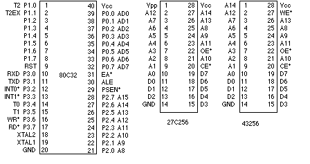
Pinouts
Here are the pinouts for the 3 main chips:
Be carefull - it is totally unforgiving of underflowing stacks.
The compiler works as a normal applicatioon from a Unix or MPW (Mac) shell, or DOS prompt. It takes commands
in the format:
asm51 [-Bm] [-o output] input
If you omit the output filename it takes the input file name and changes the extension to '.51' which
contains an Intel Hex formatted download image - suitable for sending to the onboard monitor
or for sending to a ROM burner. The -m flag is used it creates a link map/symbol table, if the -B flag is included it outputs a Perl program to stderr that will convert all the ajmp/ljmps to the correct types to same the most space (you may have to do this several times before
it converges). While I've had no problems I have been told that the Intel Hex output of the assembler is refused by some ROM
burners - if you have problems try converting all the lower case hex to upper case and see if that fixes the problem.
        .=0x8000
send_vector     = 0x86                  ;; pointer to send routine
entry:  mov     r7, #str>>8		; string base address
        mov     r6, #str&0xff
loop:           mov     dph, r7		; get the next char from the string
                mov     dpl, r6
                movx    a, @dptr
                mov     r1, a
                jz      done		; if it's the terminating 0 character quit
                inc     r6		; inc the pointer
                acall   send		; send the char
                sjmp    loop
done:   ret				; return to the monitor

send:   mov     r0, #send_vector	; get the address of the send vector into dptr
        mov     a, @r0
        inc     r0
        mov     dpl, a
        mov     a, @r0
        mov     dph, a
        clr     a
        jmp     @a+dptr			; and jump to it

str:    db      "Hello World!\r\n"
Assemble it with "asm51 test.s" and then simply copy the test.51 file to the flight computer - how you do this depends on which program you are using to talk to it, for example on my Mac I copy the text to the clipboard in an editor and paste it into the terminal emulator window to send it. You will see a single ':' followed by another
prompt when it's done .... now type "g 8000" to the monitor to run it.References